AST Research MegaPlus II Multifunction Card Utility Software & Manual IBM PC XT
SOLD AS-IS / UNTESTED.
New when purchased 35+ years ago and stored since then.
Hardware Overview
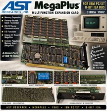
The MegaPlus II was a popular early 8-bit ISA expansion card designed primarily for the IBM Personal Computer and compatible systems. Because the original IBM PC had limited motherboard features and expansion slots, cards like this were essential for expanding memory and adding connectivity options through a single slot.
Key Components:
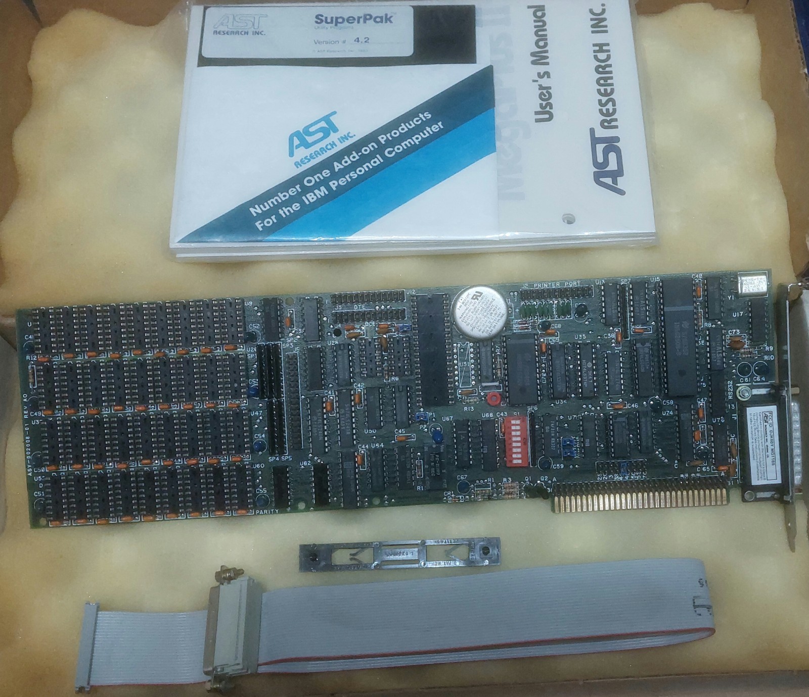
- Memory Banks: The large grid of socketed integrated circuits (DRAM chips) on the left side configuration is used to add system memory (RAM).
- Real-Time Clock (RTC): The silver circular component near the upper-middle section is the holder for a lithium coin-cell battery, which powers an onboard clock to keep the date and time when the computer is turned off.
- I/O Connectivity: The board features various headers and integrated circuits to manage a parallel printer port, an RS-232C serial communication port, and optional expansion headers.
- Configurable DIP Switches: The red block with white toggles near the bottom-middle allows the user to configure system memory addresses and communication port assignments manually.
Documentation & Software
- MegaPlus II User's Manual: The official documentation package from AST Research Inc. detailing configuration, jumper settings, and installation steps.
- SuperPak Utility Software: The manual mentions version 4.2 software, which historically included SuperDrive (a RAM disk simulator utility) and SuperSpool (a print spooler utility) designed to let users maximize the utility of the extra RAM.
Here is an in-depth, detailed technical breakdown of the hardware components, design, and architecture of the AST Research MegaPlus II expansion card
1. Board Layout & Structural Architecture
- Interface & Form Factor: This is a full-length 8-bit ISA (Industry Standard Architecture) card, characterized by the gold-plated edge connector along the bottom right. It was designed to slide into the expansion slots of the IBM PC (Model 5150) and IBM PC XT (Model 5160).
- PCB Manufacturing Details: On the far-left edge of the green fiberglass printed circuit board, the printed silk-screen text reads ASSY-002008-01 REV A0, which identifies the specific engineering revision and assembly number of this PCB layout.
2. Memory Architecture (Left Block)
- DRAM Array: Nearly half of the card's surface area is dedicated to a dense matrix of socketed Dual In-line Package (DIP) DRAM chips.
- Parity Support: At the very bottom of this memory section, there are markings for PARITY, indicating that the memory layout includes the extra 9th bit required for hardware error checking, matching the strict standards of original IBM PC architectures.
- Upgradability: The sockets allowed users to progressively upgrade their system RAM. Depending on the density of the chips used (typically 64-kilobit chips), these banks could add up to 256 Kilobytes of memory directly on the primary board, with further expansion possible via a secondary piggyback card.
3. Integrated Real-Time Clock (Center-Right)
- Battery Holder: The circular silver component at the top-middle is a coin-cell battery retainer (typically holding a CR2032 or similar 3V lithium cell).
- The RTC Subsystem: Original IBM PCs did not have a built-in clock and would prompt users to type the date and time manually at every boot. The hardware circuit tied to this battery allowed the computer to automatically remember the system time between power cycles using AST's included utility software.
4. Configuration & Logic Blocks (Center & Bottom-Right)
- DIP Switch Block: The prominent red component with 8 small white toggle switches near the bottom-center is used to configure hardware addresses manually. These switches map out the memory start addresses, assign COM port IRQs, and prevent hardware conflicts with other expansion cards.
- Logic Gates and Controllers: Surrounding the switches are various logic chips (like the 74-series TTL logic family) that handle address decoding, bus buffering, and signal timing between the ISA slot and the onboard components.
5. Input/Output (I/O) Interfaces & Peripherals (Far Right)
- On-Board Serial Port: Located near the top-right text labeled RS232, this circuitry manages serial communications (such as connecting a modem or a serial mouse).
- Printer Port Routing: Silk-screened text labels like PRINTER PORT near the top indicate the internal headers used to route a parallel printer interface.
- External Bracket Assembly: The metal bracket on the far right secures the card to the computer chassis. It includes a standard DB-25 male connector natively exposed to the back of the PC.
- Ribbon Cables & Extra Ports: The gray ribbon cables and secondary metal slot bracket lying at the bottom of the image are used to expand the card's physical ports. Since only one port fits on the main bracket, these ribbon cables plug into the internal pin headers (like the GAME port header or a second serial port) and route them to an adjacent empty slot on the back of the PC